TP — Building a RISC-V Processor
Overview
Introduction
In this exercise, you will implement parts of the data path of a simple single-cycle implementation of the RISC-V base ISA in logisim. The encodings of the instructions to be implemented can be found in this document. A detailed documentation of all basic instructions can be found on this website.
Constraints and hypotheses
The goal of this exercise is not a realistic processor implementation, even if at the end you will be able to run a real RISC-V binary on your model. The goal is to deepen you understanding of the principals of processor design, and the role and interconnection of the different components that make up a processor core. In order to make things easier, there are a couple of constraints and hypotheses throughout this exercise:
- We will be only using 16 registers instead of the full 32. This corresponds to the RV32E variant, where E stands for embedded. This is to reduce the logic of the register bank.
- While addresses have a size of 32 bits, we will only use the lower 16 bits to address instruction and data memories. Regarding the simple test programs we are using, this is not a real restriction (64k ought to be enough for anyone), just be sure not to use higher addresss in your tests.
- As presented in the lecture, we will use memories with asynchronous read, i.e. the read data is available in the same cycle in which we present the address. For larger memories, this is not realistic, but needed here in order to build a single-cycle core.
Setup
Download the archive with the logisim sources and unpack it somewhere in your home directory:
tar xzf tp-riscv.tar.gz
cd tp-riscv/riscv
Register-to-register Data Path
For this exercise, you will be starting from a circuit template that already implements the basic data path for register-to-register instructions. However, neither the instruction decoding nor the ALU are finished. Starting from the root of the archive, change into the riscv subdirectory:
cd riscv
logisim riscv-r.circ &
But before you start to play with the circuit, let's look at the data path:
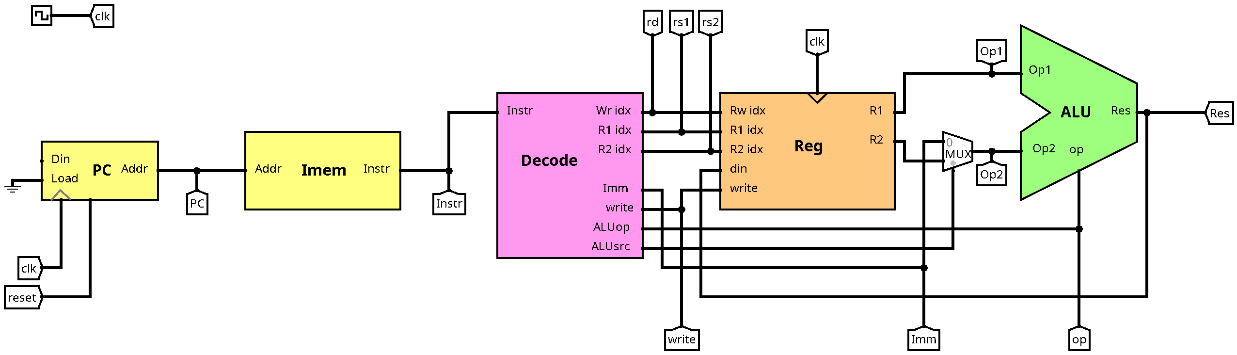
This should by now look familiar to you. Upstream in the data path, there is the program counter (PC). For now, it only counts by steps of four (each instruction is four bytes). The Load and Din inputs will come in handy later for jumps and branches. The output of the PC is connected to the instruction memory (Imem), which outputs the corresponding instruction word in the same cycle. Next in the data path comes the decode unit (Decode), which decomposes the instruction in order to command the remaining components: The register bank (Reg) and the arithmetic-logic unit (ALU). You can inspect and change the subcircuits by either right-clicking on them (View) or by double-clicking on them in the circuit list on the left hand side of the window. Note that some components are imported from external libraries and are not supposed to be changed (the register bank and the instruction memory).
Note that there are many labels on the different connections (called tunnels in logisim). On the one hand side, this is for documentation purposes. On the other hand side, tunnels can be used to avoid big ugly knots in the wiring: All tunnels with the same name will carry the same value throughout simulation. Feel free to use tunnels for your implementation in order to keep things readable. They can be found in the Wiring category. Note that all tunnels of the same name must have the same size, otherwise logisim will highlight them in orange and show a message on "incompatible widths".
Another component frequently used in this exercise are splitters, which can be used in both ways: splitting a multi-bit signal into single bits (or subvectors) and composing individual bits to a multi-bit signal. Splitters can also be found in the Wiring category in case you need them.
Simulating the Processor
As in previous exercises, there are two ways to simulate the processor in order
to help you debug your design. For both ways, the first thing we need is some
interesting input for the processor, in other words some machine code. If you
look into the asm subdirectory, you will find a few test programs in
assembler. They are compiled automatically during the build into a textual format that can be
read by logisim in order to initialise the instruction memory. To build the memory images, switch into the riscv subdirectory and call
make
This will produce some files ending with .mem which contain the machine code in hexadecimal format. This is how you can load one of these programs from within logisim:
- Right click on the Imem circuit instance, and choose View Imem. This will open a view of the internals of the instruction memory.
- Right click on the circuit component in the middle of the schema (the actual memory), and choose Load Image.
- In the file dialog, select the appropriate
.memfile
Alternatively, you can also edit the memory content by hand: just choose Edit Contents instead of Load Image. You can now start simulating the circuit by advancing the clock signal with control-T. If this does not work, you might need to enable simulation: There is a tick box in the Simulate menu of logisim for this. Note that whenever you reset the simulation (control-R), the contents of the memory are lost and you need to reload them from the file.
Alternatively, the Makefile also provides rules to run simulations from the command line, procuding wave traces that can be inspected with GTKWave. Executing make in the riscv directory will produce a wave trace for each exercise. For example, in order to view the trace for the register-to-register data path, call
make test_r2r
The trace files are stored in the vcd subdirectory. You can also open them directly with GTKWave:
gtkwave vcd/test-r2r.gtkw
Implementing the ALU
The first thing you are going to do is implementing the ALU. For the purpose of this exercise, here is an overview of the operations that must be supported:
| short name | description | value |
|---|---|---|
| ADD | Addition | 0000 |
| SLL | Logical left shift | 0001 |
| SLT | Set less than | 0010 |
| SLTU | Set less than unsigned | 0011 |
| XOR | Bitwise exclusive or | 0100 |
| SRL | Logical right shift | 0101 |
| OR | Bitwise or | 0110 |
| AND | Bitwise and | 0111 |
| SUB | Subtraction | 1000 |
The short names of the operations are actually identical to instruction names in the RISC-V base ISA, which is not surprising, since these instructions perform the corresponding operations. They should however not be confused with instructions, since the ALU operation is coded in four bits, while the instructions are 32 bit wide. Furthermore, We will see later that other instructions (such as memory loads or branches) will make use some of these operations, too.
Now open the ALU circuit and start implementing these nine operations. You can use any of the available library elements of logisim (note that there are such predefined circuits for all of them).
Implementing the Decode Unit
Now that you have completed one of the core elements of the data path, let's switch to the decode unit in order to feed the ALU with some real data. Let's have a look at the interface of the decode unit. It is a combinational circuit that takes the current instruction word as input and outputs
- The indices of the registers to be read: R1idx and R2idx
- The index of the register to be written (if applicable): Wridx
- A signal to indicate if the above register should be updated: write
- The ALU operation to be applied: ALUop
- An immediate value: Imm
- A signal selecting between the immediate (0) and the second register (1) to be fed into the ALU: ALUsrc
Let's have a look into the Decode circuit:
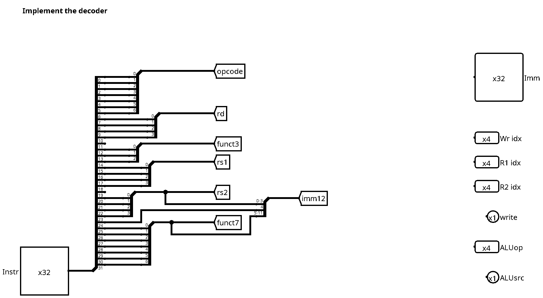
For now, it basically consists of splitters which decompose the instruction words into the different subfields according to the ISA specification of the basic instruction formats[^rv32e]. It is now up to you to use these fields in order to feed the outputs of the decoder unit with the correct values.
In a first step, you will implement the following register-to-register instructions: add, sub, sll, slt, sltu, xor, srl, or, and. These corrspond exactly to the implemented ALU operations. All of them take two registers as input and write the result to a register. Here is the encoding of the add instruction:

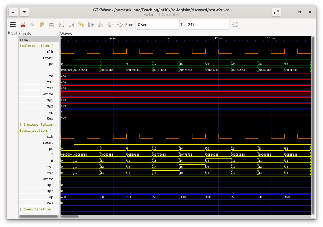
In order to test your decoder, you can run the following command in the riscv directory:
make test_r2r
This will show a wave trace with your simulation and a correct specification trace:
Immediate Instructions
As you can see in the above trace, there is not much computations going on,
since all the register values are zero. How do we start up the processor in
order to use some interesting values? The answer is immediate instructions.
These instructions perform computations between one source register and an
immmediate constant encoded in the instruction word, storing the result in a
register. In this step, you will implement the instructions addi, slti,
sltiu, xori, ori, andi, slli, and srli. Note that there is no subi
instruction, since we can use immediate addition and change the sign of the
immediate value. Here is the encoding of the xori instruction:

These are the changes that you need to make in your design:
- The signal ALUsrc must no longer be a constant, but choose between the immediate value or the second source register
- Connect the 12 bit immediate value from the instruction (sign extended) to the imm output of the decoder
You can test your implementation with the following command:
make test_imm
This test executes the program in asm/test-imm.asm, which mixes
register-to-register and immediate instructions. Compare your trace to the
specification trace in order to debug your circuit.
Load Instruction
Our circuit starts to resemble a real processor. The next thing we are going to add is the load instruction lw (load word). Instead of feeding immediate values to the registers, we can define a data section in the assembler code and load those values from the memory. Here is an example program (you can find it in the file asm/test-load.asm):
main:
	li s0, %lo(tab)  # s0 <- &tab
	lw a0, 0(s0)     # a0 <- MEM[s0]   (= tab[0])
	lw a1, 4(s0)     # a1 <- MEM[s0+4] (= tab[1])
	add a2, a0, a1   # a2 <- a0 + a1
	nop
	nop
	nop
	nop

	.align 4
tab:
	.word 0xcafe0123
	.word 0x5a5a5a5a
The second and third instruction are loads. lw a0, 0(s0) loads a memory word into register a0, where the address is computed as the value of register s0 plus a constant offset, which is zero in this case.
There is another new instruction in this code, namely
li. This is actually a pseudo instruction, which is not part of the machine code specification, but will be translated by the assembler into valid instructions. In this case,listands for load immediate, and it serves to initialise a register with a constant value. Depending on the size of the constant value, it will be translated into one or several machine code instructions. In the above program, we make use of another feature of gcc's RISC-V assembler, which is the%lomacro. During assembly, it will be replaced by the lower 16 bits (a half word) of the address that the argument (the labeltab) corresponds to. Since we using small addresses which fit into 16 bits, theliinstruction will be replaced by theaddiinstruction.
Here is the instruction encoding of the lw instruction:
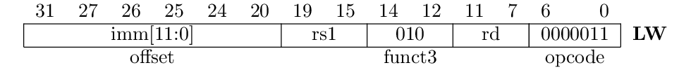
Its format is identical to the immediate instructions, so hopefully we can reuse a lot of the things that are already in place.
Let's look at the data path needed to implement the load word instruction. As
before, there is a template circuit, which needs to be completed. In the riscv
directory, open the circuit riscv-load.circ with logisim. With respect to the previous exercise, there is only a slight difference: We have added an output signal to the decode unit, the signal load. Otherwise, there is space left on the right hand side of the ALU in order to add the data memory. Note that otherwise the decoder and the ALU already implement register-to-register and immediate instructions. This is what's left to do in order to do loads:
- Add the data memory to the data path. You can find it in the dmem category on the left hand side of the window.
- Connect the address input and the data output of the memory to the appropriate signals. You might need to add extra logic in order to correctly feed the register to be written (what are the possible inputs?).
- Complete the decoder unit.
For the last item, there are several changes: The added load signal, the ALU operation to be performed (signal op), and the selection of the second ALU operand (signal ALUsrc). All of those need to take into account the new lw instruction.
You can test your implementation with the build target
make test_load
Store Instruction
Loading is nice, but storing is even nicer. Here is the encoding of the sw (store word) instruction:
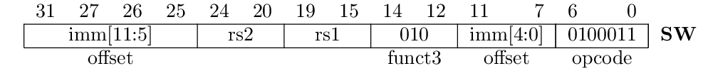
This instruction has the S format, where there is no destination register (we are writing the memory instead), but two source registers: The first one (rs1) is used for the address calculation, while the second one (rs2) is the register to be sent to the memory. The immediate field -- needed for the address offset -- is cut into two pieces in order to keep the position of the register addresses at the same place within the instruction word. Otherwise, the address calculation is the same as for the load instructions.
Open the file riscv-loadstore.circ and complete the data path in order to
implement the sw instruction. There is a new signal produced by the decoder
unit (store), indicating a memory store instruction. Otherwise, the circuit
already implements all register-to-register and immediate instructions as well
as the lw instruction. Here is what you need to do:
- Complete the data path by connecting the inputs Wdata and write of the data memory with the appropriate signals
- Complete the decode unit
For the decoder unit, the following changes need to be made:
- Implement the store signal
- Complete the write signal (we have now the first instruction which does not write the register bank)
- Complete the ALUsrc and op signals for the address calculation (same as for loads)
- Complete the imm calculation, taking into account the modified position of the immediate bits in the S-type format
You can test your circuit with the build rule
make test_store
The test executes the following program (see the file asm/test-loadstore.asm):
main:
	li s0, %lo(tab)  # s0 <- &tab      (Res = 0x0030)
	lw a1, 0(s0)     # a1 <- MEM[s0]   (Res = 0x000f)
	addi a1, a1, 1   # a1 <- a1 + 1    (Res = 0x0010)
	sw a1, 0(s0)     # MEM[s0] <- a1   (Res = 0x0030)
	addi a1, a1, 1   # a1 <- a1 + 1    (Res = 0x0011)
	sw a1, 4(s0)     # MEM[s0+4] <- a1 (Res = 0x0034)
	nop
	nop
	lw a1, 0(s0)     # a1 <- MEM[s0]   (Res = 0x0010)
	lw a2, 4(s0)     # a2 <- MEM[s0+4] (Res = 0x0011)
	nop
	nop

.align 2
tab:
	.word 0x000f
Branches
The RISC-V base instruction set has six different branch instructions, all of which share the same format and opcode. Here is the encoding of the blt (branch if less than) instruction:

The above encoding corresponds to the B-type instruction format, which is very similat to the S-type format of store instructions. The only difference is the immediate value, which is somewhat twisted (but don't worry, we already implemented the decoding for you). All branch instructions compare two registers (addressed by rs1 and rs2), where the type of the comparison is given by the funct3 field. If the condition is true, then the instruction will execute a jump to a relative address, which is calculated by adding the immediate offset value to the current PC value. Note that target addresses are always multiples of 2, and thus the immediate value does not encode the least signigicant bit, which is always zero. In this way, we can encode signed offsets of 13 bits.
We have already implemented one of the branch instructions, namely blt. Open the file ricscv-branch.circ in logisim. Compare the data path with the load-store version from the previous exercise:
- What does the new component BU do?
- How is the comparison realised?
Here is a short program that is used to thest the branch implementation:
main:
	li   a0, 0x80
	li   a1, 0x70
loop:
	addi a1, a1, 2
	blt  a1, a0, loop
	nop
What does the program do? You can simulate the circuit executing the above program with the build rule
make test_branch
Look at the generated trace and try to understand what is happening. Once you have fully understood the implementation of blt, try to implement at least one additional branch instruction:
beq: branch if equalbne: branch if not equalbge: branch if greater or equalbltu: branch if less than unsignedbgeu: branch if greater or equal unsigned
You might need to add new operation to the ALU for some of the instructions. Feel free to modify the branch unit, possibly adding new input or output signals. You will need to modify the test program in the file asm/test-branch.asm in order to validate your implementation.
[^rv32e] Note that the register indices only take four bits, since we are using the RV32E variant with 16 registers only.