Solution - Sequential Logic
Overview
D Flip-Flop with Enable
In order to add an enable signal to a flip-flop, let's consider the state of the circuit (i.e. the value of the flip-flop's output signal Q):
- If enable is 1, the state will be updated to the value of D
- If enable is 0, the state will remain unchanged, i.e. keep the current value of Q
So basically, we need to choose among two different input signals to set the new state. The basic circuit element to implement such a choice is a multiplexer. We can therefore use the following structure to realise the enable:
Now we want to add a synchronous reset to the above circuit. The reset should be considered to be of higher priority than the enable signal: If both reset and enable signals are active, we want the reset to take precedence such that Q will be reset to zero. This can be realised by adding an AND gate behind the multiplexer. In this way, the output of the multiplexer will be overridden by 0 if reset is active:
Addressable Register
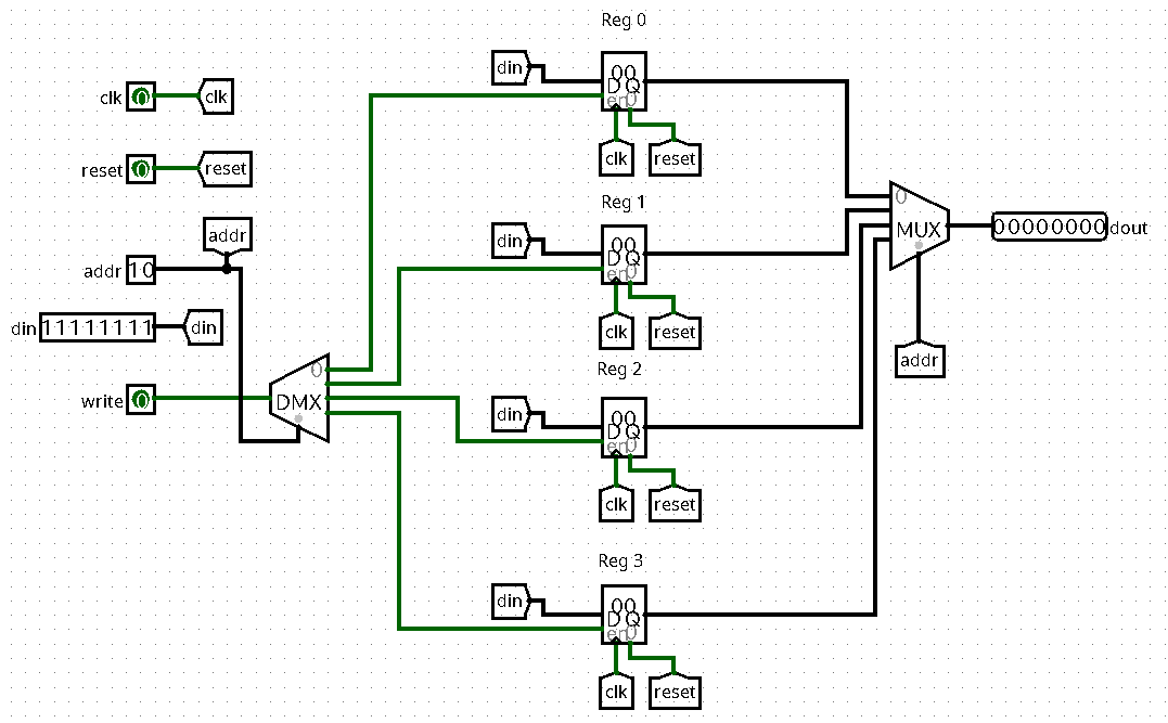
Question 1: The component that we need to implement the reading logic is a multiplexer. Depending on the value of the address input, we want to forward the output value of the addressed register to the circuit's output dout. The multiplexer can be found in the Plexers category in LogiSim. The correct parameters are 8 data bits and 2 select bits.
Question 2: What we need is the possibility to set exactly one of the enable inputs of the registers to 1 and the others to 0, where the active enable signal corresponds to the one chosen by the address input. There are basically two possibilties: The first one uses a 1-to-4-decoder (we have seen this circuit in the lecture) in order to produce four signals one of which is active. In order to cover the case where the write input is 0, we need to add an AND gate with write and each of the four outputs in order to produce the four enable signals for the registers.
The second (and simpler) solution uses a 1-to-4-demultiplexer, which does both of the above at the same time. It distributes a single signal (in our case write) to four distinct signals, depending on an address input. Both the decoder and the demultiplexer can be found in the Plexers category in logisim.
Here is the complete circuit using a demultiplexer for the writing logic. Note that it uses labels in order to avoid excessive wiring:

Serial to Parallel Conversion
The circuit structure needed to implement the parallalisation of the serial input is a shift register, where we tap the outputs of the individual registers in parallel:
There are different solutions for the valid output: We can either use another shift register with a single 1 is shifted from the input to the output such that it arrives at the output at the moment when four inputs have been processed, and start over again. Another solution is to use a counter that counts the number of processed input bits:
Note that normally we would need to count to four, since this is the number of processed input bits for a complete output word. However, we will process a new bit in the same cycle when we output the parallel word, so we can use a two bit modulo counter, comparing it value with 3. We only need to delay the output of the comparator in order to synchronise it with the input sequence. Here is a complete timing diagram that shows how the circuit works:
Counters
For the basic version of the counter, there is not much to do. We just need to wire up the circuit as in the figure below:
In order to implement saturation arithmetics, we need to stop counting once we reach 15, and instead keep the current value of the counter register. This is basically the same mechanisme as the flip-flop with enable:
In the above circuit, once the output of the comparator goes high, the multiplexer will feed the current state of the counter back to the register, until the circuit is reset.
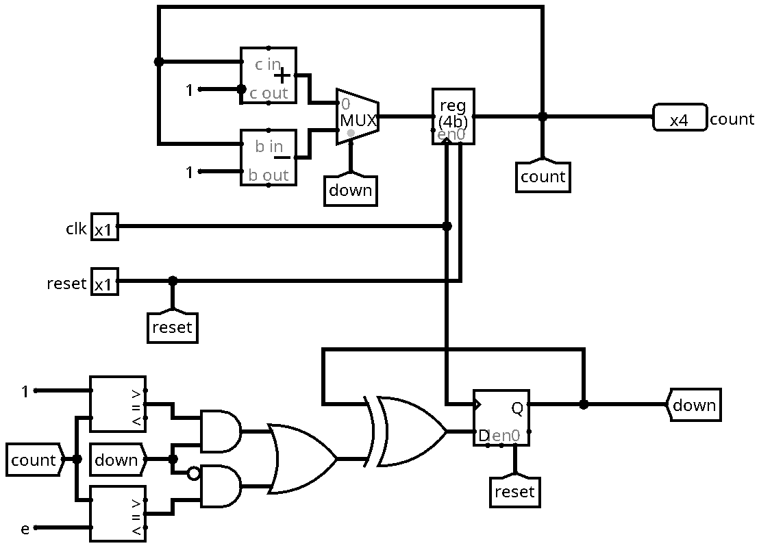
In the last exercise, the task was to realise an up-and-down counter. The first thing to notice is that besides the register holding the value of the counter, we need an additional information: Since during the incrementing phase and the decrementing phase we go through the same numbers, the circuit needs another input that decides if we shall add or subtract one from the current value. This information can be represented by a single bit, let's call the signal down:
Instead of an input, down needs to be an internal state of the circuit. We will store it in a single flip-flop. Let's think about the next state function that will determine the value of down in the next clock cycle, depending on the current state of the circuit (including the counter value and down itself): We will start counting up. Once we reach the value 15, we will start decrementing. Note however that we must not wait until we actually reach 15 before flipping down, since its value is stored in a register, so the value used by the multiplexer is delayed by one cycle. We need to decide one cycle before reaching the maximum (respectively the minimum) to switch the counting direction. Here is a truth table showing the above idea:
| Q | down | n_down |
|---|---|---|
| < 14 | 0 | 0 |
| 14 | 0 | 1 |
| > 1 | 1 | 1 |
| 1 | 1 | 0 |
Here, n_down is the next state of down. Here is a possible Boolean equation:
\[ \text{n_down} = \text{down} \oplus (\overline{\text{down}} \cdot (\text{count}=14) + \text{down} \cdot (\text{count}=1)) \]
Below is the screenshot of a logisim circuit that implements the above equation:
