How to Build a Processor
Now that we know how a program looks like at the lowest level, broken down into its machine code instructions, let's look at how these instructions are actually executed. In the following, we will construct a simple single cycle processor (meaning that each instruction is executed within a single clock cycle) implementing (parts of) the RISC-V base ISA.
How to Execute a Program
In order to execute a program, it needs to be available in machine language, loaded into the main memory. The processor will then execute the instructions one by one1. The execution of a single instruction can be boiled down to the following steps:
- Read the instruction word from memory (fetch)
- Determine the type of the instruction and its operands (decode)
- Perform the demanded computations (execute)
- Store the result in the requested location (write back)
- Determine the next instruction and start again
The internal structure of our future processor implementation will roughly follow the above execution phases. Starting with the basic building blocks, we will proceed phase by phase.
Basic Components
Let's look back at the global architecture of a computer:
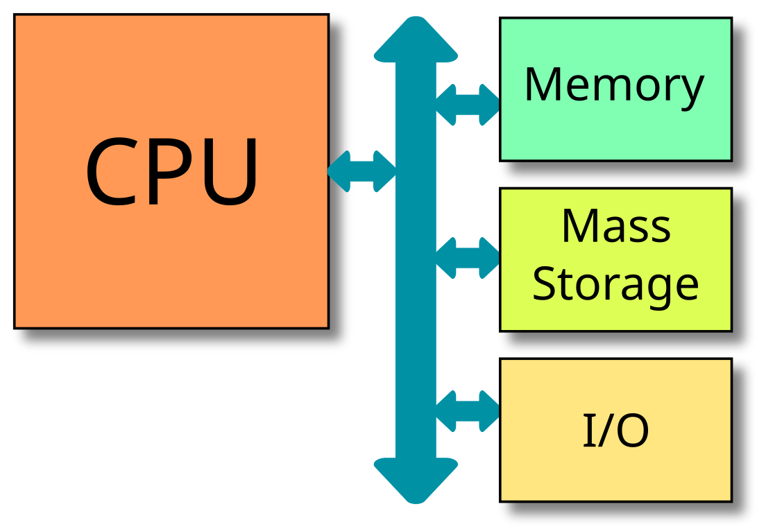
In this lecture, we will not consider mass storage devices or peripherals. We will concentrate on the CPU itself and the memory, or rather memories.
Memories
In fact, for the purpose of designing our processor, we will make the assumption that we have two distinct memories: One holding the instructions, and one holding the data. This assumption is quite convenient, since we may need to do two memory accesses during the execution of one instruction (such as an instrucion loading data from memory). With a single shared memory, this would be very complicated. A computer with distinct memories for instructions and data is also called a Harvard Architecture, in contrast to the von Neumann Architecture which has a single shared memory. In reality, the distinction is not that important, and many of nowadays processors are somewhat in between the two: While the processor core has distinct interfaces (i.e. connetions or wires) for instructions and data, they both finally lead to a single shared memory. We will come back to this topic in the second part of the lecture, when we talk about the memory layout of a C program.
The instruction memory (IMem) will be represented as a simple block like this:

It takes as input an address of an instruction to fetch (IAddr) and returns the instruction word stored at this address (Instr). Both signals are 32 bits wide. The instruction memory is byte addressed. Since each instruction has a size of four bytes (32 bits), we assume that IAddr is aligned to the beginning of an instrucion, i.e. that it is a multiple of four.
For simplicity, we will also assume that read accesses to the instruction memory are asynchronous (or combinatorial), which means that the instrucion is returned in the same clock cycle. The instruction memory does not allow write access.
The data memory (DMem) is represented by the following symbol:

It takes as inputs an address of the data to be read or written (DAddr), the data to be written (WData), and a control signal (write) that indicates if we are performing a read acess (write = 0) or a write access (write = 1). In case of a read access, the memory outputs the data (RData) stored at the given address. As for the instruction memory, read accesses are combinatorial. In contrast, write accesses are synchronous: As indicated by the small triangle on the bottom of the DMem block, there is a clock input (the clock signal itself is omitted here and in the following). The update of the data memory will take place at the following rising edge of the clock. Just like IMem, the data memory is byte addressed.
Registers
Our processor needs to hold a certain amount of information as its internal state. When we talk about registers, we are usually referring to the processor's working memory, also called general purpose registers. They can be accessed directly by the instructions. However, as we have learned in the chapter on sequential logic, register is actually just the term for one or several D flip-flops that store some information. In our implementation, there is one special register, which holds the address of the current instruction. It is generally called the program counter (PC). This term is not very accurate, since it does not really count programs. A better name would be instruction pointer, but we will stick with the historical term. The PC is represented by the following symbol:

At its output, it reflects the current instruction's address (IAddr). At each rising edge of the clock (again, the clock signal is omitted here), it is updated with a new value, the next instruction's address (nIAddr). At startup, the PC is initialised with the address 0.
Coming back to the working memory of the processor, the general purpose
registers, their interface is more complex. As has been explained in the
previous chapter on the RISC-V instruction set, most instructions work on those
registers. And, as demonstrated with the add instruction, there can be up to two
source registers (the operands) and one destination register (to store the
result). Since our processor shall execute each instruction in one clock cycle,
we must be able to read two registers simultaneously, and write one register at
the same time. Here is the symbol of the register file (the component containing
all the registers):

We will not discuss the internals of this component, just its functionality: There are three register addresses, two for reading and one for writing. The addresses are called indices here just in order to distinguish them from 32 bit wide memory addresses. Since there are 32 registers (as specified by the RISC-V base ISA), each index must be 5 bits wide. As for the data memory, we have an additional input to provide the data to be written, and a control signal that indicates wether the current instruction writes the destination register. On the output side, there are two read data outputs for the respective source registers. The temporal behavior of the register file is as usual: Reading is combinatorial, and writing takes place at the following rising edge of the clock.
Let's get started with the first phase: fetch.
Fetching Instructions
In order to give our processor something interesting to do, we need to feed it with a new instruction at each clock cycle. With the basic components presented above, we have everything we need for this purpose: The PC indicates the address of the current instruction, and the instruction itself is stored in the IMem. So all we need to do is to connect these two components together, feeding the output of the PC into the IMem. The only thing that is missing is the next instruction's address (nIAddr). For now, we will execute all instructions one after the other, so PC should take on the values 0, 4, 8, 12, etc. This can be realised by a 32 bit adder circuit that adds the constant value 4 to the current IAddr in order to compute nIAddr. Here is our fetch phase in action:
In the animation you can see the first four clock cycles, fetching the beginning of the example machine code in the previous section:
| Cycle | Address | Instrucion |
|---|---|---|
| 0 | 0x00 | 0xFF010113 |
| 1 | 0x04 | 0x00112623 |
| 2 | 0x08 | 0x00812423 |
| 3 | 0x0C | 0x01010413 |
Decoding
Now that we are able to fetch instructions from the memory, what do we do with them? Well first of all, we need to decode them. While during the last phase of the compilation process, we have painfully encoded our program in machine language, we now need to reverse this process by extracting meaningful values from the packed machine instructions. Fortunately, the design of the RISC-V instruction set makes the decoding relatively easy for most instructions, at least in terms of logic complexity. At this point, we will only explain the basic principle, the concrete decoding function will evolve with the different instruction classes discussed later in this chapter.
Let's look again at the add instruction:
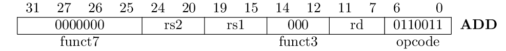
Remember the information we find in the instruction encoding:
- What shall the instruction do?
- What are the operands of the requested operation?
- Where to put the result?
Now in the circuit implementation of our processor, we have a 32 bit signal coming from the instruction memory which carries the current machine instruction to be executed, meaning that we have an individual wire for each bit of the above encoding. So in order to decode the instruction, we need to look into the values of the individual bits and groups of bits in order to understand what the instruction is supposed to do. Here is another view of the instruction, which emphasises this fact:
Here, we only consider register-to-register instructions, which all share the same opcode (0110011). In this case, the position and meaning of the remaining fields are fixed, and all we need to do is to redirect packets of bits to the downstream components in the data path, in particular the register file and the arithmetic and logic unit (ALU), which we will explain shortly. Indeed, the packets of 5 bits corresponding to the source and destination registers can directly be used as inputs for the register file (for the read and write indices, respectively). Later, when we start adding more and more instruction classes, the decoding logic will become more and more complex, and additional combinatorial logic will be needed beyond mere redirecting of signals.
Execution
Now that we know where to get the operands from and where to put the result, the remaining question is what to do with the data? In the RISC-V base instruction set, there is a certain number of different operations that we can perform, among others addition, subtraction, comparison, bit-wise or, bit-wise and, etc. For all these different operations, there will be one central component in our processor, called the arithmetic and logic unit (ALU). At this point, we will not discuss about its internal implementation (which will be left as an exercise), but only present its global interface and functionality. The ALU is a combinatorial circuit block. It has two 32 bit operand inputs and one 32 bit result output. The performed operation is controlled by an additional input op, which needs to be provided by the decode phase. We will discuss the concrete values for this signal in the following chapters. Here is the circuit symbol that we will use for the ALU:
Note that the bit size of the operation control signal depends on the number of different operations that the ALU implements.
Write Back
Once the ALU has done its job, we need to store the result. For now, all register-to-register instructions write the result into a register. Its index is given by the rd field of the instruction word, which we have already extracted during the decode phase. So all we need to do is to redirect the output of the ALU back to the Write data input of the register file, and to set the Write control signal of the register file to constant 1. Here is the corresponding part of the data path:
Putting it all together
In this section, we have presented the basic functionality of a processor and how it executes an instrucion. We have discovered the basic components needed to implement it, and some simple interactions between the components. In the following sections, we will dive even deeper into the understanding of the RISC-V instruction set and its implementation by a single cycle processor. We will discuss the different instruction classes and how to modify and extend the data path in order to be able to execute these instructions.
Modern processors actually execute many instructions in parallel, but the basic steps are the same.