Part 1 - From Logic Gates to Processors
In the first part of this lecture, we build a simple processor from scratch. We start with the very basic building blocks: Logic gates. We show how to combine simple combinatorial gates in order to construct arithmetic operators. Going one step further, we introduce sequential logic, which is needed in order to memorize data and to realize complex sequential behavior.
From combinatorial logic to arithmetics
In this chapter, we will introduce the notion of combinatorial logic by presenting the basics of Boolean logic, the basic logic functions as well as some more complex but often used logical functions. We will see how to represent numbers and how to perform arithmetic operations on those numbers. Finally, we will introduce the concept of propagation time in logic operations.
Boolean logic
Introduction
Let be the two-element set .
A logical variable is an element of . It has only two possible values: or (which can also be interpreted as false or true, respectively).
A logical function is a mapping from to which maps an -tuple of logical variables , often called inputs, to a logical variable , often called output.
There are two categories of logic functions, depending on their temporal behavior.
A combinatorial function is a logical function for which the output depends only on the current state of the inputs:
A sequential function is a logical function for which the output depends on the current state of its inputs but also on their past states:
In this chapter, we will deal only with combinatorial functions. Sequential functions will be introduced in the chapter Sequential logic.
Representations of logical functions
There are several methods to describe a combinatorial logical function. These methods are all equivalent and the choice of one or the other will only depend on the context of use.
Truth table
The first method consists in listing, for each of the possible values of its inputs, the value of the function’s output. This list, very often presented in the form of a table, is called truth table.
The major drawback of this method is that this table can be very large. Indeed, if the function takes as input logical variables, it takes rows in this table to list all the possible values of the inputs.
Example of a truth table of a function taking as input two logical variables and :
Example of a function taking two logical variables as input
and
Analytical equation
This method consists in giving the equation of the output of the function based on its inputs. The list and meaning of operators will be given in the section on basic logic functions. You will learn more about the way we can manipulate and simplify Boolean equations in the section on Boolean Algebra.
Example of a function taking three logical variables as input and : .
Schematic representation
This method consists of graphically representing a Boolean function using nodes with standardised symbols 1 for basic functions and edges to indicate the connection of an output to an input.

Functional description
This method consists in describing, in natural language, the behavior of the output according to the inputs of the function.
Example: the output is 1 if, and only if, at least one of or is 1.
Hardware description language
This method consists in describing the function in a particular language, called Hardware Description Language — HDL, easily understood by a computer. There are several HDLs auch as SystemVerilog or VHDL. In this course, we are not going to consider HDLs, you will encounter them in the second semester.
There are several standards to represent these basic functions. In this course, we will use the "American" standard (from ANSI 91-1984) because it is one of the most used. There is also a "European" standard (IEC 60617-12).
Basic logic functions
This section presents the basic logic functions, also called logic gates, which will be used later on in order to construct more complex functions.
The Inverter (NOT)
Description
The output is if and only if the input is .
Truth table
| e | s |
|---|---|
Equation
Another common symbol to denote the negation of a variable is .
Symbol

The AND Gate
Description
The output is if and only if both inputs equal . 1
Truth table
| a | b | s |
|---|---|---|
Equation
In this lecture, we use the operator to denote conjunction (the AND operation). It is not to be confused with multiplication of integers or reals. But, as will become more clear in the next chapter, both share some common properties. Another common symbol for the conjunction is .
Symbol

The OR Gate
Description
The output is if and only if both inputs equal .2
Truth table
| a | b | s |
|---|---|---|
Equation
In this lecture, we use the operator to denote disjunction (the OR operation). It is not to be confused with addition of integers or reals (again, both share some common properties). Another common symbol for the conjunction is .
Symbol

The NAND (not AND) Gate
Truth table
Description
This is the complementary function of AND. The output is if and only if both inputs equal .
Truth table
| a | b | s |
|---|---|---|
Equation
Symbol

The NOR (not OR) Gate
Description
This is the complementary function of the OR. The output is if and only if both inputs are .
Truth table
| a | b | s |
|---|---|---|
Equation
Symbol

Exclusive OR (XOR)
Description
The output is if one, and only one, of the two inputs is . 3
Truth table
| a | b | s |
|---|---|---|
Equation
Symbol

Exclusive NOT OR (XNOR)
Description
This is the complementary function of the exclusive OR. The output is if and only if both inputs are equal.
Truth table
| a | b | s |
|---|---|---|
Equation
Symbol

The AND function can also be interpreted as a function of forcing a signal to zero: in the expression , the signal is equal to only if , otherwise it is 0.
The OR function can also be interpreted as a function of forcing a signal to one: in the expression , the signal is equal to only if otherwise it is 1.
The exclusive OR function can also be interpreted as a selection function between a datum and its complementary: in the expression , the signal is equal to if otherwise it is
Boolean Algebra
Just as with integers or real numbers, there are certain laws that help us manipulate expressions, in order to simplify them or to prove them equivalent. Most of the following laws should be familiar to you, and it should now become clear why we chose and for conjunction and disjunction, respectively. In the following, and are Boolean variables.
Laws for disjunction and conjunction
For the two monotone operators and , the following laws apply:
Associativity
Commutativity
Neutral elements
Annihilation
Idempotence
Distributivity
Absorption
Non-monotone Laws
If we add negation, these additional laws apply:
Complementary
Double negation
De Morgan
Showing Equivalence with Truth Tables
In order to show that two Boolean terms are indeed euqivalent, we can just establish their truth tables and compare them line by line. Let's show the first De Morgan law for example:
| 0 | 0 | 0 | 1 |
| 0 | 1 | 1 | 0 |
| 1 | 0 | 1 | 0 |
| 1 | 1 | 1 | 0 |
And the right hand side:
| 0 | 0 | 1 | 1 | 1 |
| 0 | 1 | 1 | 0 | 0 |
| 1 | 0 | 0 | 1 | 0 |
| 1 | 1 | 0 | 0 | 0 |
From Truthtable to Boolean Expression
Now if we want to do the reverse, how can we come up with a Boolean equation from a truth table? Consider the following truth table:
| 0 | 0 | 0 |
| 0 | 1 | 1 |
| 1 | 0 | 1 |
| 1 | 1 | 0 |
Disjunctive Normal Form
We can read each line of the truth table as follows: If is zero and is zero, then is zero; if is zero and is one, then is one; etc. We can represent each line as a conjunction (also called product), such as for the first line, for the second line etc. Now in order to get a one at the output, at least one of the conditions for a one must apply. In other words, we can take the disjunction (the sum) of the products of all the lines leading to a one at the output:
This form of Boolean expression is called sum-of-products (SOP) form, or disjunctive normal form (DNF). Each complete product term (in which all of the variables appear), is also called a minterm. The above recipe works for any Boolean function with variables. However, since it starts with a truth table and translates each line leading to a one, the resulting expression is of exponential size (in ) in general.
Conjunctive Normal Form
As a matter of fact, we can also use the remaining lines of the truth table, those leading to zero, to construct a Boolean expression. We just need to negate the respective minterms and take the conjunction. Intuitively, we are saying that if none of these "forbidden" minterms applies, then the result must be one, otherwise it will be zero. Consider again the truth table from the beginning of the section. Starting from the first and last line, we obtain:
Applying De Morgan's law on each negated minterm, we obtain:
This form of Boolean expression is called product-of-sums (POS) form or conjunctive normal form (CNF).
Rewriting and Logic Minimization
Instead of establishing the truth tables for two Boolean expressions, we can also apply the laws of Boolean Algebra in order to transform (rewrite) one expression into the other one symbolically. As an example, let's show that the DNF and CNF we just derived are indeed equivalent, starting with the CNF:
Another application of this rewriting is logic minimization. Indeed, if we want to create a combinatorial circuit from a Boolean function specification, each operator in the Boolean expression will become a logic gate. If we find an equivalent expression with less operators, this will lead to a cheaper implementation. Instead of rewriting expressions manually, there are several algorithms that can be used for systematic and automated logic minimization, such as Quine McCluskey or Karnaugh maps. The study of these algorithms is beyond the scope of this lecture.
Important logical functions
The basic logic gates seen in the previous section allow us to construct any combinatorial logical function. In this section, we will introduce some commonly used functions.
The multiplexer
A multiplexer 1 with inputs is a logical function whose output is equal to one of its inputs. The choice among the inputs is made through a particular selection input.
Two Input Multiplexer
The simplest multiplexer is the two-input multiplexer. The following symbol is used for this function:

If the input is , the output of the multiplexer will be equal to the value presented on the input . Similarly, if is , the output will be equal to the value presented on the input .
The truth table of the two-input multiplexer is as follows:
The behavior of this multiplexer can also be described by the following equation:
N-input multiplexer
We can generalize and have multiplexers with inputs. In this case, it requires selection inputs in order to choose among one of the inputs.
For example, the 4-input multiplexer:

whose equation is:
This multiplexer can be constructed using three 2-input multiplexers as follows:

The Decoder
A decoder is a logic function with inputs and outputs 2 among which one, and only one, output is , the index of this active output being the value present on the input, considered as a integer encoded on bits (see Natural numbers about the representation of natural numbers).
Example: 2 to 4 Decoder
The truth table for the 2 to 4 decoder is:
The logic equations of the outputs are as follows:
Sometimes also called a switch function
We also use the terminology to decoder, example: 2 to 4 decoder
Representation of numbers
So far we have only dealt with logical variables and performed logical operations. We will see in this section how to represent and manipulate numbers.
Natural numbers
General Representation
A natural number can be represented in a base by a -tuple such that 1:
In this representation:
-
is a digit of rank and belongs to a set of symbols ( to )
-
is called the most significant digit
-
is called the least significant digit
The most commonly used bases2 are:
-
: decimal representation,
-
: hexadecimal representation,
-
: octal representation,
-
: binary representation, . A binary digit is also called bit (short for binary digit)
Unsigned binary representation
We will focus in the following on the representation of numbers in binary (base 2). In this base, an unsigned integer can be represented by the -tuple such that:
Where:
-
is a bit (it belongs to a set of symbols: or )
-
is called the most significant bit (MSB)
-
is called the least significant bit (LSB)
Conversion between hexadecimal and binary
It is very simple to go from a number represented in hexadecimal to a number represented as an unsigned binary. Just concatenate the 4-bit binary representation of each of the hexadecimal digits.
Example:
We have:
Similarly, to go from an unsigned binary representation to a hexadecimal representation, it suffices to group the bits 4 by 4 (starting from the least significant bits), thereby transforming each of the groups into a hexadecimal digit.
Example:
Modulo binary representation
In practice, in hardware, numbers are represented and manipulated over a finite fixed number of bits. So a number will be represented, modulo , on bits. Using bits, it is therefore possible to represent the natural numbers in the range ].
Signed integers
There are several methods to represent signed integers. The most commonly used is the representation in two’s complement (CA2).
As seen previously, using bits, numbers are represented modulo , i.e. has the same representation as , has the same representation as , etc.
If we extend this principle to negative numbers, we would require to have the same representation as (i.e. ), that has the same representation as (i.e. ), etc.
By convention, in the 2’s complement representation, the numbers whose most significant bit is 1 will be considered as negative numbers, and the numbers whose most significant bit is 0 will be considered as positive numbers3.
In two’s complement, we can therefore represent, using bits, the signed numbers in the range ].
Example: 4-bit representation ():
| CA2 Binary | Decimal | Unsigned Binary | Decimal |
|---|---|---|---|
From a mathematical point of view, a number represented as two’s complement with bits by is given as:
Sign extension
Extension rules allow us to go from a number represented with bits to the same number represented with bits.
Unsigned integers
In the unsigned case (natural numbers), the extension consists of adding bits valued on the left (most significant bits).
Example: represented as an unsigned integer using bits gives us . Using bits, it is represented as .
Two’s complement
In the case of a signed number represented in two’s complement, the extension is a little more complex because we must not forget that the most significant bit carries the information of the sign. For a two’s complement number, the extension is done by duplicating the most significant bit.
Examples: is represented with bits in two’s complement in the form . On bits, it is represented as . is represented with bits in two’s complement as . On bits, it turns out as .
Proof: Let be a signed integer represented in two’s complement using bits.
Hence is its representation with bits.
Summary
In conclusion, when we represent a number in binary, it is very important to specify the convention chosen (unsigned, two’s complement, fixed point…) as well as the number of bits.
Note that the operators and take on their classical mathematical meaning here, i.e. addition and multiplication, unlike in the previous chapter where they corresponded to the logical operators OR and AND.
In the following, in case of risk of confusion, the base in which a number is represented will be indicated as a subscript, example: , ,
This keeps compatibility with the unsigned representation
Fixed because once the respective number of bits of the integer part and the fractional part are fixed, they do not change. There are other methods, including the floating-point representation — which you’ve probably heard of — which is significantly more complex to implement at the operational level and which we will therefore not discuss in this course.
Arithmetic operators
In this section, we will learn how to perform addition and subtraction on binary numbers (unsigned or in two’s complement), using basic logic gates introduced in the #sec:basic-logical-functions[1.2] section.
Addition
Introduction
It is possible to add two binary numbers using the basic algorithm [^11] consisting of adding each digit of the two operands from the least significant bit to the most significant bit and propagating the carry bit.
Example: Unsigned addition of and
Elementary adder
In fact, we are performing several elementary additions taking as inputs a bit of each of the two operands of the calculation ( and ) and an input carry () from the preceding elementary addition, and producing as output a bit of the result () and an output carry () for the next elementary addition.
This elementary addition can be written arithmetically as the equation[^12]:
The two outputs and being Boolean variables, it is possible to express their value in the form of Boolean functions of the inputs , and . The truth table of this elementary addition operator is as follows:
| Decimal | |||||
|---|---|---|---|---|---|
From an analytical point of view, we obtain the following equations[^13]:
The one-bit adder can be represented by the following diagram:

Adding complete numbers
To realize a complete addition over several bits, we just connect together elementary 1-bit operators[^14]:

Dynamics of the addition
We need to pay attention to the fact that the addition of two unsigned binary numbers (two’s complement numbers, respectively) on bits produces a result that can be represented as an unsigned number (two’s complement number, respectively) on bits.
In order to be assert a correct result when adding two unsigned numbers represented respectively with and bits, we first expand the two operands to bits (using the extension rule seen previously in section #sec:rules-extension[1.4.3]). The result, which is unsigned, will be represented on bits. The possible output carry is to be discarded.
Similarly, in order assert a correct result when adding two numbers represented respectively with and bits in two’s complement, we need to extend the two operands to bits (using the sign extension rule seen earlier in section #sec:rules-extension[1.4.3]). The result will be represented as bits in two’s complement form. The outgoing carry of the addition is to be discarded.
Subtraction
We can also perform a subtraction of two numbers using one-bit elementary subtractors.
Basic subtractor
From an arithmetic point of view, we have[^15]:
The corresponding truth table is:
| Decimal | |||||
|---|---|---|---|---|---|
From a logical point of view, if we express the outputs ( and ) depending on inputs and elementary logical functions, we obtain[^16]:
This one-bit subtractor can be represented by the following diagram:

[^11] Algorithm you learned in primary school
[^12] The and the here represent the arithmetic operators of addition and multiplication.
[^13] The and here represent the operators logic OR and AND.
[^14] This structure is called a carry-ripple adder. There are other adder structures offering trade-offs between the number of logical gates and computation time.
[^15] The and the represent the arithmetic operators addition and multiplication here.
[^16] The and the represent the logical operators OR and AND.
From propagation time to computation time
Because of the physical constraints related to its concrete implementation, the output of a logic gate does not change its state instantaneously when its inputs change.
The propagation time of a gate, denoted by , is the time between the change of the value of an input and the stabilization of the value of the gate’s output.

During this time, the value of the gate output may not correspond to the logical function applied on the gate’s current input values. The output value should therefore not be taken into account during this period.
Taking this propagation time into account is important in order to determine the maximum operating speed of the implementation of a logic function and more generally the computation time of any arithmetic function.
Example of the 1-bit adder
Consider again the 1-bit full adder (as introduced in section Addition):
If we assume that each of the basic gates (here the XORs with two inputs, two-input AND and three-input OR) all have a propagation time of , once the inputs , and are stable, the outputs will be stable and correct after 2 ns. The propagation time of this implementation of the 1-bit adder is therefore 2 ns.
Example of the carry-ripple adder
From this 1-bit adder, we construct a simple adder with carry propagation:
Once the inputs , and are stable, the outputs and of the first 1-bit adder will be stable after 2 ns. As the input of the second 1-bit adder is only stable after 2 ns, its outputs and will be stable 2 ns later, i.e. after 4 ns.
So for this 4-bit carry-ripple adder, the outputs and will finally be stable after 8 ns. The propagation time, or computation time, of this adder is therefore 8 ns.
Sequential logic
In this chapter we will introduce synchronous sequential logic, starting with the notion of memorisation. We then present the D flip-flop, the principal memorising element used for the implementation of synchronous logic, as well as the timing constraints to guarantee its correct operation. Finally, we will present some applications of synchronous logic.
Synchronous sequential logic
Memorisation and sequential logic
The combinatorial logical and arithmetic operations presented in the previous chapter all share the following property:
- For the same value of the inputs, we always obtain the same output value. In other words, the combinatorial operators have no memory.
We need to keep in mind that these operators have a propagation time that must be respected to be sure that the output result is valid.
How can we use these operators in order to chain several consecutive calculations reliably?
Take as an example the combinatorial function in the figure below:

The block has three inputs , and , and a single output . If we change one of the inputs, we have to wait for the result to be valid.
We want to chain several calculations and obtain the following sequence:
-
-
-
-
…
It must be ensured that the inputs are not modified as long as the output is invalid. However, if the inputs stem from the outside world or from a another computational block, we do not have the guarantee that they remain stable.
Thus, we need to add specific circuit elements in order to capture the values of the inputs and prevent them from changing during the computation, as shown in the following figure:

To simplify the task, capturing and storing the inputs will be done at the same time, synchronously.
Once we are sure that the result is valid (after ), we can capture the output result and at the same time present new values on the inputs. The output, thus captured, can in turn be used as input for another computational block.
All of this is summarised in the following figure:

We have the following sequence:
-
at the time instant the inputs are captured (we also say sampled)
-
at the output of the combinatorial block is valid
-
at the output is sampled and new input values captured
-
And so on …
This logic is called sequential synchronous logic. We have the guarantee that the computations are correct as long as the interval between the sampling instants is greater than the propagation time of the combinatorial block.
In the following, we will see which component is used to sample and memorise the signals and how we synchronise the sampling times.
The D flip-flop
The basic component of synchronous sequential logic is the D flip-flop. It can also be called dff, just flipflop and sometimes register.
Figure formalpara_title shows the schematic of a D flip-flop. The D flip-flop has two inputs and one output:
-
A particular input, the clock clk symbolized by a triangle.
-
An input for the data, D.
-
An output for stored data, Q.
The clock clk is used to synchronise all the flip-flops in a circuit. The sampling of the input signals takes place on the rising edge of the clock signal.
Circuit symbol of a D flip-flop

The operation of the D flip-flop can be described as follows:
-
At each rising edge of the clock clk (transition ) input D is copied to output Q. We say the data is sampled.
-
Between two clock edges, the output Q does not change, it is memorised.
This behavior can, as for combinatorial logic, be represented by a truth table (see Truth table of a D flip-flop).
| D | clk | Q | effect |
|---|---|---|---|
| (copy of D on Q) | |||
| (copy of D on Q) | |||
| Q | (Q keeps its value) | ||
| Q | (Q keeps its value) | ||
| Q | (Q keeps its value) |
Truth table of a D flip-flop
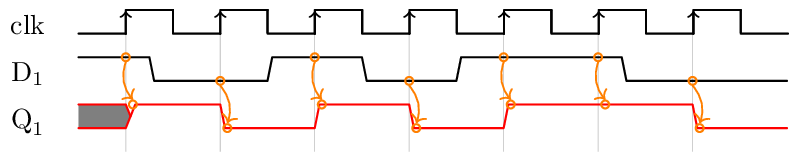
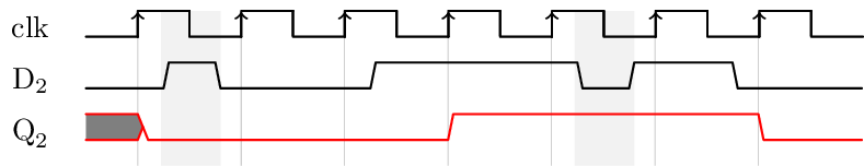
Using D Flip-Flops
1. Sampling:
A D flip-flop is used to sample the input data. As can be seen on the following timing diagram, the value of input D is captured at each rising edge of the clock. This value is kept until the next rising edge.
2. Filtering:
A D flip-flop filters transient input changes that occur between clock edges. As indicated the following timing diagram, the changes on the input signal which take less than the clock period do not appear on the output.
Registers
As we often manipulate words (or vectors) of several bits, we will use several flip-flops together. This assembly of flip-flops is called a register.
The symbol of a register is the same as that for a D flip-flop. The size of the register (i.e. the number of bits) is indicated on the input and output of the register:

Initialisation
The initial state of a D flip-flop, when the voltage of the circuit is turned on, is not known. It depends on several factors, including:
-
the technology used to manufacture the circuit,
-
the internal structure of the flip-flop,
-
technological variations between the elements of the same circuit,
-
ambient noise…
In order to obtain a predictable behavior, we need to be able to initialise the flip-flops to a known state. For this, an additional control signal must be used. This particular signal will allow us to force the initial state of a flip-flop.
If the initial state is 0 we speak of reset. If the initial state is
1 we speak of preset.
In the following, we will only consider what is called a synchronous reset. It is effective at the clock edge. Note that the asynchronous reset will be treated in a different lecture in the second semester. A reset can be:
-
positive: initialise the flip-flops when it goes to
1 -
negative: initialise the flip-flops when it goes to
0
It is good practice to add the letter "n" to the name of a reset signal if it is
a negative reset, such as n_reset.
The following figure shows how one can build a flip-flop with a negative synchronous reset:

The timing diagram shows the operation of a synchronous reset:
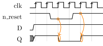
The n_reset signal is of negative polarity, it acts on the flip-flop
when its value is 0. At the following edge of the clock, the flip-flop
is forced to zero. When the n_reset signal returns to 1, the
flip-flop regains its normal operation and the input data is sampled at
the following edge of the clock.
A synchronous reset must follow the same rules as any signal sampled by a D flip-flop.
In general, a synchronous reset is used to functionally initialise parts of the circuit. It is thus generated by another part of the circuit which is also synchronous, which guarantees that it has a duration of at least one clock period.
Generalization
A generic block of sequential logic is represented in the following figure:

In a block of sequential logic the same clock is used to synchronise all computations. All input signals from the outside world must be sampled. Outputs of combinatorial logic blocks must also be sampled.
These outputs can be:
-
used externally (in another block),
-
or redirected to the inputs of the combinatorial logic.
In the second case we speak of an internal state. The value of the outputs then depends on the value of the inputs and this internal state.
In order for the consecutive output values to be predictable, we must be able to force the initial state. This is done thanks to an external reset signal.
Applications of synchronous logic
In the following, You will find some example applications of synchronous logic.
Shift registers
The following figure shows a shift register made up of four D flip-flops connected serially. This structure is called a shift register with a depth of 4:

The shift register has signal E as input and signal S as output. intermediate signals , and are used to link the output of a flip-flop to the input of the flip-flop that follows it.
The following timing diagram shows the operation of the shift register:

At the first clock tick, the input E is copied to . Then at the following clock ticks, the value of E is shifted from one flip-flop to the next.
Using a shift register
A shift register can be used to delay a signal by an integer number of clock periods. In the previous example, the output S is a copy of input E with four clock periods of delay.
In the same way, the outputs of the flip-flops represent the history of the signal E.
Counters
A counter is an important building block for synchronous sequential logic. The counter’s output is incremented every clock cycle. In order to build a counter we need two elements:
-
a register storing the value (state) of the counter,
-
an incrementer (an adder with one of its inputs tied to ) to calculate the next value.

The above figure shows the schematic of such a counter using an 8-bit register and adder. The initialisation signal reset_n allows to force the initial state and to start counting from zero. Then, at each stroke of the clock, the value of Q is incremented. Since the size of the register and the adder is 8 bits, once the counter reaches 255, it will naturally wrap around to 0 in the following cycle. This is also called a modulo counter.
The following timing diagram shows the evolution of the signals in the counter. Here the reset signal is a synchronous one:
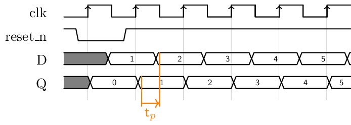
Note that the reset signal acts on the output of the register. Notice also that the output of the adder changes after the output of the register, showing the propagation time of the combinatorial logic.
The pipeline
The pipeline is a technique which makes it possible to increase the operation frequency of a sequential block. It is useful in order to increase the throughput of a data stream.
Consider the following example:

-
A combinatorial function with propagation time
-
Data is presented on inputs A and B at the rate of the clock clk with period .
Note: To simplify the expressions, we neglect in this example the propagation time of the registers.
The system works correctly as long as the following relation between the clock period and the propagation time is satisfied:
The output of the combinatorial block C is sampled and we obtain a result on the output OUT once in every period , as shown in the following timing diagram:

We now decompose into two combinatorial functions and with the respective propagation times and .
- We take care to have and
The point represents the set of signals linking the two combinatorial blocks and :

The system works properly as long as
In the following timing diagram, we have set to be able to compare it to the previous diagram:

Let’s add a register between the combinatorial blocks and . Both blocks are now preceded and followed by registers:

One also says that we have added a pipeline stage.
The system is working properly if the following two conditions are met:
But since the two propagation times and are less than initial propagation time , we can reduce the period of the clock . Or in other words, we can increase the operating frequency and therefore the rate at which the calculations are made1. The new situation is illustrated in the following timing diagram:

Let’s summarize:
-
The pipeline allows to increase the operating frequency.
-
The initial latency increases by the number of pipeline stages.
-
The complexity and size of the circuit has been increased by adding flip-flops and by modifying the initial combinatorial block.
Notice that the first result arrives at the OUT output after two clock periods.
Building a RISC-V Processor
In this chapter, we will finally put things together: Based on the combinatorial and sequential circuits from the previous chapters, we will construct a simple processor. After a brief introduction to the basic notions of computer architecture, we will discuss the language understood by a processor: the machine language. In the following, the basic architectural elements of a single-cycle processor will be presented. Wiring up these elements in the right way will allow us to execute different types of instructions: Starting with register-to-register instructions, instructions for memory access will be added subsequently, followed by some more complex instructions. The chapter ends with an overview on the RISC-V assembly language.
Introduction
In this section, we will explore the basic components that a computer is made of. We are particularly interested in the Central Processing Unit (CPU), also known as the processsor. We will introduce the notion of a processor's architecture and present different trade-offs found in today's computing systems.
What's inside a computer?
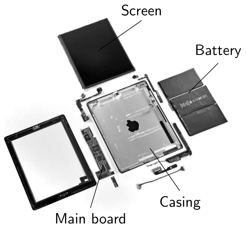
The figure below shows the typical organisation of the different components found inside a computer:
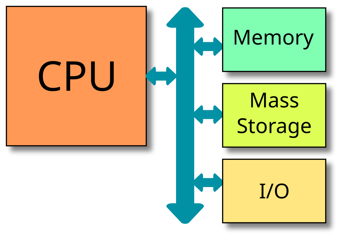
The Central Processing Unit (CPU) is connected via a system bus (in blue) to the main memory and the peripherals, including possibly mass storage devices (hard disk, flash memory, optical storage devices), and input/output peripherals. Among the latter, depending on the specific computer, we can find
- Keyboard
- Mouse or touchpad
- Screen display
- Audio input and output
- Network devices (WiFi, ethernet)
- Fingerprint sensor
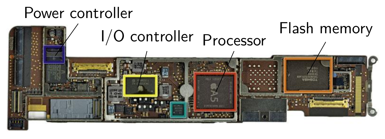
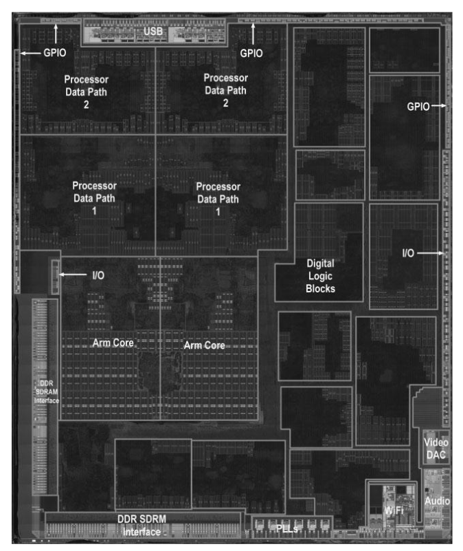
and many more. Note that the above figure shows only the logical connection between the different components. There might actually be several different busses for different purposes, for example a low speed serial bus for connecting keyboard and mouse, and a high speed parallel bus to connect to a video accelerator. Also, some connections might be realised by cables or copper lines on the main board, while other components will be integrated together with the CPU on the same integrated circuit, such as the network controller. In this case, we also talk of a system on chip (SoC).
The Central Processing Unit
The CPU is the place where the main load of computations take place. The CPU receives input data from the memory and the input peripherals, processes it, and sends the results back to the memory or to the output peripherals. In this section, we will give a brief overview of the way a processor does its job, before explaining how we actually build a processor.
A processor can accomplish very complex tasks, such as showing this website, having a video conference with your parents, or playing SuperTuxCart. But the actual operations performed by the processor are very simple, such as adding two numbers or copying a value from one place to another. It can just execute many such operations very fast. One elementary operation is called an instruction. The type of instructions and the form of the processed data depend on the specific processor's architecture. This will be discussed in the next section.
Processor Architectures
When we talk about a processor's architecture, we are actually talking about different aspects. In many cases, we are referring to its Instruction Set Architecture (ISA). The ISA determines the set of elementary operations, also called instructions, which the processor is able to understand and execute. This is a fundamental aspect, since everything we want the computer to do must be expressed in terms of these mostly very simple instructions. Here are some examples of more or less popular ISAs, some of which you might have heard of:
- x86 is a family of ISAs originally developed by Intel, starting with the 8086 processor, released in 1978. It is still alive today in Intel's latest x86-64 desktop processors.
- ARM is a family of ISAs developed by ARM. It is used ranging from low-power embedded systems, mobile phones, and more recently also in desktop computers, such as Apple's M1 and M2 processors.
- RISC-V is an open standard ISA developed at the University of California, Berkeley. Started as an academic standard, there are more and more (mostly small embedded) RISC-V processors fabricated by various vendors1.
An important architectural parameter is the register size, which can be thought of as the size (in bits) of data (such as integer numbers) that a processor can naturally deal with. When we talk about 8-bit, 32-bit, or 64-bit architectures, we are really referring to this size. This means for example that a processor with a 32-bit architecture will be able to add two 32-bit signed integers with a single instruction. If we want to add bigger numbers, we need to implement this in software, thereby using several instructions. Most of the cited ISA families above offer different sizes. For example, ARM offers 32-bit ISAs for low-power micro-controllers and more powerful 64-bit ISAs for mobile phones or desktop applications. RISC-V has also 32-bit and 64-bit variants. In historial computers or in small embedded systems, we can find 8-bit architectures such as the 6502 ISA in the Commodore 64 or Atmel's AVR architecture in the original Arduino boards.
Finally, the architecture can also refer to the internal organisation of a specific processor design: the way it actually realises the different instructions of its ISA in hardware. In this context, we also talk about the processor's micro-architecture. The job of a computer architect is to propose such an organisation in order to fulfil the requirements in terms of complexity (the number of logic gates used), performance (the number of instructions that can be executed per time unit), and other aspects such as power consumption, security, resistance against faults etc.
The choice of the ISA has many implications, both for the applications (their development, their performance, ...) as well as the underlying hardware (its complexity, its power consumption, its performance, ...). This will be illustrated by three examples:
For most embedded systems, such as small electronic devices running on battery power, available resources are limited. This includes the physical size or volume, electrical energy, and memory space. In the same time, their functionality is usually well-defined and consists mostly in simple control tasks. The architecture of choice will therefore be as simple as possible. ARM and RISC-V are examples of such ISAs.
In contrast, general purpose processors (GPPs), such as the one in your laptop, have a wide range of applications, including audio and video, gaming, text processing, internet browsing, and software development. Historically, Intel has been dominating the market for processors in desktop computers. The x86 ISA has seen several extensions over the years, adding special instructions for example for vector or matrix computations, virtualization, or cryptography. The goal of a GPP is to have a high average performance for many different applications. However, due to the sheer number of supported instructions, modern x86 processors are extraordinarily complex. The high power density of the fabricated chips requires active cooling.
Nowadays, some embedded systems allow for multimedia applications such as audio playback or image classification while still depending on battery power. In some of these cases, it might be a good choice to use a specialized instruction set architecure, which provides some special operations suitable to accelerate the needed functionality. For audio and video applications, a digital signal processor (DSP) can be used, either as a standalone processor, or in combination with a standard micro-controller. Examples of DSP architectures are PIC24 or MSC81xx. Typically, DSPs offer additional arithmetic instructions for floating point or fixed point numbers. The goal is to have a sufficient performance for the needed functionality, while minimizing complexity and power consumption.
The acronym RISC in RISC-V stands for reduced instruction set computer, as opposed to complex instruction set computer (CISC). It opposes ISAs with few and simple instructions to those having rich and complex instructions.
The Machine Language
In this section, we will look into the language understood by the processor - the machine language - and present how the processor executes a program.
As discussed in the previous section, each processor is able to execute a particular set of instructions, depending on its ISA. But how do we actually talk to the processor, telling it which instructions it should execute? While as (future) engineers, we mostly think of algorithms and programs in a symbolic form (including types and variables), the processor at the hardware level has no idea of such things. It only understands instructions in a very concrete form, called the machine language, in binary format: ones and zeros.
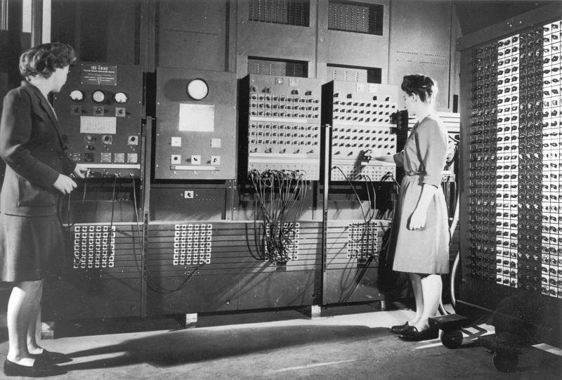
In ancient times, this was more or less the level of abstraction on which computers were programmed: By connecting cables and setting switches. The photo above shows two programmers (Betty Jean Jennings and Fran Bilas) operating the ENIAC computer in 1946.
From a high level language to machine language
Nowadays, nobody would want to write machine language any more. Instead, we write programs in dedicated languages such as C or OCaml. A special program -- the compiler -- is used to translate programs from high level languages down to the machine language of a specific target architecture. We will not go into the details of the compilation process here1, you will learn more about it later in this and other lectures. But let's have a quick look at the different levels of abstraction.
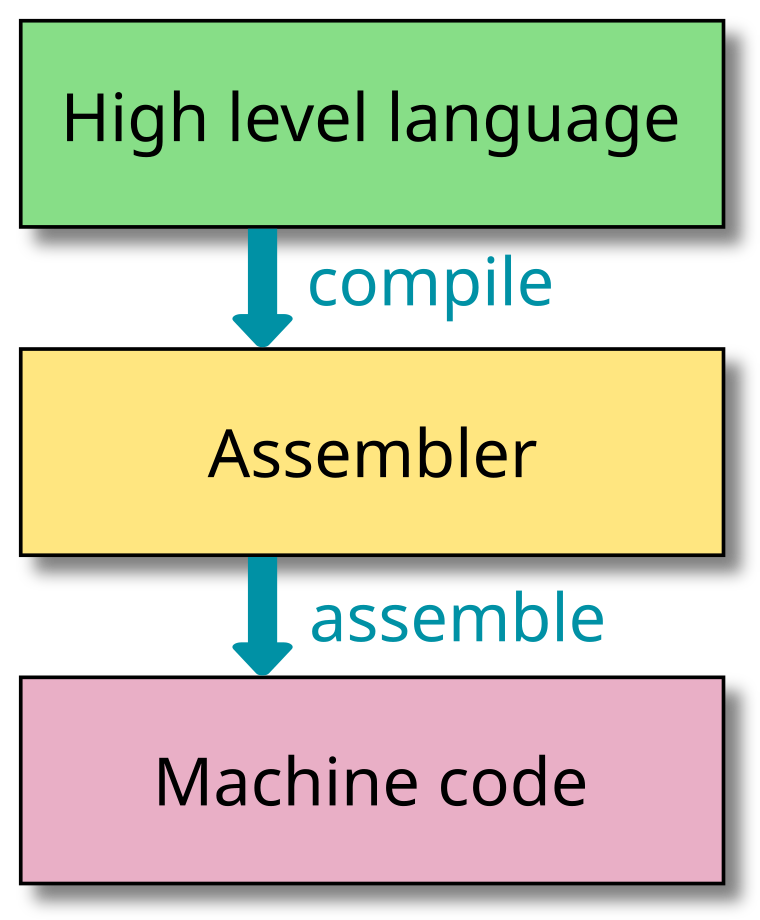
The above figure shows the basic steps in the compilation: We are starting from a high level programming language. At this point, the program is given in an abstract form: It does not know about the concrete hardware architecture it will run on. This has the advantage that programs written in a programming language are mostly portable: They can be run on computers with different ISAs. The basic elements in most programming languages are variables and functions. As an example, here is a small snippet of C:
int square(int x) {
    return x * x;
}

int main() {
    int x = square(42);
}
Without diving into the concrete syntax of C, this program basically computes the square of 42, which you have probably guessed without much of a headache. The first step is compilation, which translates the generic code to another language, called assembler. While the assembler code is still human readable, the representation is already specific to a certain ISA: It uses mnemonic forms of the ISA's instructions and registers, symbolic labels, as well as different textual representations of literals (constant values):
square:
   addi  sp,sp,-16
   sw    ra,12(sp)
   sw    s0,8(sp)
   addi  s0,sp,16
   sw    a0,-16(s0)
   lw    a1,-16(s0)
   lw    a0,-16(s0)
   call  __mulsi3
   mv    a5,a0
   mv    a0,a5
   lw    ra,12(sp)
   lw    s0,8(sp)
   addi  sp,sp,16
   jr    ra
   .align   2
main:
   addi  sp,sp,-16
   sw    ra,12(sp)
   sw    s0,8(sp)
   addi  s0,sp,16
   li    a0,42
   call  square
   sw    a0,-16(s0)
   li    a5,0
   mv    a0,a5
   lw    ra,12(sp)
   lw    s0,8(sp)
   addi  sp,sp,16
   jr    ra
The above code shows the same program in RISC-V assembler. There are two labels
(main and square), otherwise there is one instruction per line of
code. Each instruction starts with the instruction name (such as addi),
followed by its arguments. The arguments can be one or more registers (such as
a0 or sp), a constant, or a label, depending on the instruction.
There is a fixed number of registers, each of which can hold 32 bits of data:
function arguments, intermediate results, return values, or addresses. The
registers constitute the working memory of the processor. They have no type, the
programmer needs to know which kind of data she is manipulating.
The second step in the compilation process -- also called assembler -- resolves any symbolic labels and directives and produces the final machine code. Here is a hexadecimal representation of the machine code for the above program:
ff010113  00112623  00812423  01010413
fea42823  ff042583  ff042503  00000097
000080e7  00050793  00078513  00c12083
00812403  01010113  00008067  ff010113
00112623  00812423  01010413  02a00513
00000097  000080e7  fea42823  00000793
00078513  00c12083  00812403  01010113
00008067
Instruction types
Looking back at the assembler code that resulted from the compilation of the squaring program, we find different types of instructions, each of which accomplishes a simple task. A first class of instructions are those performing arithmetic and logic operations. Examples are addition (such as the addi instruction in the code), subtraction, bitwise and, or bit shifting to the left.
A second class of instructions are memory access instructions, which move data from and to the memory. Load instructions fetch data from the memory to a register, while store instructions do the reverse: saving the value of a register to a given memory addresss. Examples in the assembler code are the lw (load word) and sw (store word) instructions.
A third class is formed by instructions that change the control flow of the program: jumps, branches, and calls. While jumps are unconditional, branch instructions depend on a condition, such as the value of a register being zero or not. Calls are jumps which additionally store the address of the current instruction in a register, in order to be able to return there later. This is how function calls are realized in hardware. In the assembler code, we can find the jr (jump to register) instruction, which performs an unconditional jump to the address stored in a register.
And then there are usually a certain number of special instructions used for management or book keeping, synchronisation, or switching of privilege levels. We will not consider these instructions in this lecture.
Anatomy of an instruction
Let's have a closer look at a single machine code instruction of the RISC-V ISA. In the basic RISC-V instruction set, all instructions have the same length of 32 bits2. In order for the processor to execute an instruction, this is the information that we need to put into these 32 bits:
- What shall the instruction do?
- What are the operands of the requested operation?
- Where to put the result?
As an example, let's consider integer addition, realised by the add
instruction. In the RISC-V ISA, the operands and the result are stored in
registers, and there are exactly two operands. Considering that there are 32
registers, we need 5 bits to encode each operand register and the target
register, where the result will be stored. Here is the encoding of the add instruction:
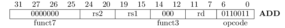
The table above shows the position and value of different fields within the instruction word. First of all, there is the opcode, located in the lower 7 bits. In case of the add instruction, its value denotes an arithmetic or logic instruction, which operates on two registers and stores the result in a register. In the RISC-V ISA, many instructions share this opcode, and the specific arithmetic or logic operation is further specified by the function fieds (funct7 and funct3). In this case, both are zero, which denotes addition. So far for the first question (what to do?).
The second question (where to find the operands?) is answered by the fields rs1 and rs2, where rs means source register. The last question (where to put the result?) is finally answered by the rd (destination register) field.
As we will see in the following chapters, many of the instructions in the RISC-V base ISA share the same format as the add instruction, they are called R-type -- or register-to-register -- instructions. We will get to know a few other formats used for branches and memory instructions. But first, we will discuss the hardware components within a processor and their interconnection, which are needed to realise such instructions.
For example, how do you write a compiler if you don't have a compiler to compile it?
There is an extension of the basic ISA, which adds compressed instructions of 16 bits.
How to Build a Processor
Now that we know how a program looks like at the lowest level, broken down into its machine code instructions, let's look at how these instructions are actually executed. In the following, we will construct a simple single cycle processor (meaning that each instruction is executed within a single clock cycle) implementing (parts of) the RISC-V base ISA.
How to Execute a Program
In order to execute a program, it needs to be available in machine language, loaded into the main memory. The processor will then execute the instructions one by one1. The execution of a single instruction can be boiled down to the following steps:
- Read the instruction word from memory (fetch)
- Determine the type of the instruction and its operands (decode)
- Perform the demanded computations (execute)
- Store the result in the requested location (write back)
- Determine the next instruction and start again
The internal structure of our future processor implementation will roughly follow the above execution phases. Starting with the basic building blocks, we will proceed phase by phase.
Basic Components
Let's look back at the global architecture of a computer:
In this lecture, we will not consider mass storage devices or peripherals. We will concentrate on the CPU itself and the memory, or rather memories.
Memories
In fact, for the purpose of designing our processor, we will make the assumption that we have two distinct memories: One holding the instructions, and one holding the data. This assumption is quite convenient, since we may need to do two memory accesses during the execution of one instruction (such as an instrucion loading data from memory). With a single shared memory, this would be very complicated. A computer with distinct memories for instructions and data is also called a Harvard Architecture, in contrast to the von Neumann Architecture which has a single shared memory. In reality, the distinction is not that important, and many of nowadays processors are somewhat in between the two: While the processor core has distinct interfaces (i.e. connetions or wires) for instructions and data, they both finally lead to a single shared memory. We will come back to this topic in the second part of the lecture, when we talk about the memory layout of a C program.
The instruction memory (IMem) will be represented as a simple block like this:

It takes as input an address of an instruction to fetch (IAddr) and returns the instruction word stored at this address (Instr). Both signals are 32 bits wide. The instruction memory is byte addressed. Since each instruction has a size of four bytes (32 bits), we assume that IAddr is aligned to the beginning of an instrucion, i.e. that it is a multiple of four.
For simplicity, we will also assume that read accesses to the instruction memory are asynchronous (or combinatorial), which means that the instrucion is returned in the same clock cycle. The instruction memory does not allow write access.
The data memory (DMem) is represented by the following symbol:

It takes as inputs an address of the data to be read or written (DAddr), the data to be written (WData), and a control signal (write) that indicates if we are performing a read acess (write = 0) or a write access (write = 1). In case of a read access, the memory outputs the data (RData) stored at the given address. As for the instruction memory, read accesses are combinatorial. In contrast, write accesses are synchronous: As indicated by the small triangle on the bottom of the DMem block, there is a clock input (the clock signal itself is omitted here and in the following). The update of the data memory will take place at the following rising edge of the clock. Just like IMem, the data memory is byte addressed.
Registers
Our processor needs to hold a certain amount of information as its internal state. When we talk about registers, we are usually referring to the processor's working memory, also called general purpose registers. They can be accessed directly by the instructions. However, as we have learned in the chapter on sequential logic, register is actually just the term for one or several D flip-flops that store some information. In our implementation, there is one special register, which holds the address of the current instruction. It is generally called the program counter (PC). This term is not very accurate, since it does not really count programs. A better name would be instruction pointer, but we will stick with the historical term. The PC is represented by the following symbol:

At its output, it reflects the current instruction's address (IAddr). At each rising edge of the clock (again, the clock signal is omitted here), it is updated with a new value, the next instruction's address (nIAddr). At startup, the PC is initialised with the address 0.
Coming back to the working memory of the processor, the general purpose
registers, their interface is more complex. As has been explained in the
previous chapter on the RISC-V instruction set, most instructions work on those
registers. And, as demonstrated with the add instruction, there can be up to two
source registers (the operands) and one destination register (to store the
result). Since our processor shall execute each instruction in one clock cycle,
we must be able to read two registers simultaneously, and write one register at
the same time. Here is the symbol of the register file (the component containing
all the registers):

We will not discuss the internals of this component, just its functionality: There are three register addresses, two for reading and one for writing. The addresses are called indices here just in order to distinguish them from 32 bit wide memory addresses. Since there are 32 registers (as specified by the RISC-V base ISA), each index must be 5 bits wide. As for the data memory, we have an additional input to provide the data to be written, and a control signal that indicates wether the current instruction writes the destination register. On the output side, there are two read data outputs for the respective source registers. The temporal behavior of the register file is as usual: Reading is combinatorial, and writing takes place at the following rising edge of the clock.
Let's get started with the first phase: fetch.
Fetching Instructions
In order to give our processor something interesting to do, we need to feed it with a new instruction at each clock cycle. With the basic components presented above, we have everything we need for this purpose: The PC indicates the address of the current instruction, and the instruction itself is stored in the IMem. So all we need to do is to connect these two components together, feeding the output of the PC into the IMem. The only thing that is missing is the next instruction's address (nIAddr). For now, we will execute all instructions one after the other, so PC should take on the values 0, 4, 8, 12, etc. This can be realised by a 32 bit adder circuit that adds the constant value 4 to the current IAddr in order to compute nIAddr. Here is our fetch phase in action:
In the animation you can see the first four clock cycles, fetching the beginning of the example machine code in the previous section:
| Cycle | Address | Instrucion |
|---|---|---|
| 0 | 0x00 | 0xFF010113 |
| 1 | 0x04 | 0x00112623 |
| 2 | 0x08 | 0x00812423 |
| 3 | 0x0C | 0x01010413 |
Decoding
Now that we are able to fetch instructions from the memory, what do we do with them? Well first of all, we need to decode them. While during the last phase of the compilation process, we have painfully encoded our program in machine language, we now need to reverse this process by extracting meaningful values from the packed machine instructions. Fortunately, the design of the RISC-V instruction set makes the decoding relatively easy for most instructions, at least in terms of logic complexity. At this point, we will only explain the basic principle, the concrete decoding function will evolve with the different instruction classes discussed later in this chapter.
Let's look again at the add instruction:
Remember the information we find in the instruction encoding:
- What shall the instruction do?
- What are the operands of the requested operation?
- Where to put the result?
Now in the circuit implementation of our processor, we have a 32 bit signal coming from the instruction memory which carries the current machine instruction to be executed, meaning that we have an individual wire for each bit of the above encoding. So in order to decode the instruction, we need to look into the values of the individual bits and groups of bits in order to understand what the instruction is supposed to do. Here is another view of the instruction, which emphasises this fact:
Here, we only consider register-to-register instructions, which all share the same opcode (0110011). In this case, the position and meaning of the remaining fields are fixed, and all we need to do is to redirect packets of bits to the downstream components in the data path, in particular the register file and the arithmetic and logic unit (ALU), which we will explain shortly. Indeed, the packets of 5 bits corresponding to the source and destination registers can directly be used as inputs for the register file (for the read and write indices, respectively). Later, when we start adding more and more instruction classes, the decoding logic will become more and more complex, and additional combinatorial logic will be needed beyond mere redirecting of signals.
Execution
Now that we know where to get the operands from and where to put the result, the remaining question is what to do with the data? In the RISC-V base instruction set, there is a certain number of different operations that we can perform, among others addition, subtraction, comparison, bit-wise or, bit-wise and, etc. For all these different operations, there will be one central component in our processor, called the arithmetic and logic unit (ALU). At this point, we will not discuss about its internal implementation (which will be left as an exercise), but only present its global interface and functionality. The ALU is a combinatorial circuit block. It has two 32 bit operand inputs and one 32 bit result output. The performed operation is controlled by an additional input op, which needs to be provided by the decode phase. We will discuss the concrete values for this signal in the following chapters. Here is the circuit symbol that we will use for the ALU:
Note that the bit size of the operation control signal depends on the number of different operations that the ALU implements.
Write Back
Once the ALU has done its job, we need to store the result. For now, all register-to-register instructions write the result into a register. Its index is given by the rd field of the instruction word, which we have already extracted during the decode phase. So all we need to do is to redirect the output of the ALU back to the Write data input of the register file, and to set the Write control signal of the register file to constant 1. Here is the corresponding part of the data path:
Putting it all together
In this section, we have presented the basic functionality of a processor and how it executes an instrucion. We have discovered the basic components needed to implement it, and some simple interactions between the components. In the following sections, we will dive even deeper into the understanding of the RISC-V instruction set and its implementation by a single cycle processor. We will discuss the different instruction classes and how to modify and extend the data path in order to be able to execute these instructions.
Modern processors actually execute many instructions in parallel, but the basic steps are the same.
Register Instructions
In this section, we will briefly describe the necessary hardware and its interconnection in order to realise register-to-register instructions. Note that the lab exercise with LogiSim will provide you with more details.
Which instructions?
In this section, we will implement R-type instructions:

This includes the following individual instructions:
- add (addition)
- sub (subtraction)
- sll (shift left logical)
- slt (set less than)
- sltu (set less than unsigned)
- xor (bit-wise exclusive or)
- srl (shift right logical)
- or (bit-wise or)
- and (bit-wise and)
All of the above instructions share the same opcode (0110011), the type of the operation is determined by the two fields funct7 and funct3.
What do they do?
Each of these instructions takes two register values, performs some logical or arithmetic computation on them and stores the result in a register.
Most of the operations should be self explaining. The two shift operations sll
and srl will shift the bits of the first register by the number of positions
indicated by the second register1.
The instruction slt (set less than) compares the two register values and
stores a 1 in the destination register if the first value is less than the
second one, otherwise it will store 0. The instruction stlu does the same but
it interprets the register values as unsigned integers.
What do we need?
There is three things that we need to implement:
- The arithmetic and logic unit (ALU), which is left as an exercise;
- The decode unit, which has already been described in the previous section;
- The wiring of the data path, putting all the components together in a meaningful way.
Let's look at the data path, described in the following.
The data path
At this point, we already have all the individual hardware components needed to realise R-type instructions. The figure below shows how they are connected and how the different parts relate to the execution phases of an instruction:
- fetch: The PC is fed into the instruction memory, returning the current instruction word.
- decode: The instruction word is split up into the individual fields.
- execute: The operands are read from the register file and sent to the ALU.
- write back: The result from the ALU is stored in the register file.
- next instruction: We add 4 to the current PC and store the value in the PC.
Note that all of the above phases happen within the same clock cycle. The next instruction address is calculated in parallel to the reading of instruction word from memory, but the PC is only updated at the next rising edge of the clock.
The term logical shift in the case of srl means that the most
significant bits will be filled with zeros. There is also an arithmetic right
shift instruction (sra), which copies the sign bit, which is consistent with
dividing the value by a power of two. The sra instruction is not treated in
this lecture.
Immediate Instructions
In this section, we will briefly describe the necessary hardware and its interconnection in order to realise immediate instructions.
Which instructions?
In this section, we will implement I-type instructions:
This includes the following individual instructions:
- addi (immediate addition)
- srli (immediate shift right logical)
- slli (immediate shift left logical)
- slti (immediate set less than)
- sltiu (immediate set less than unsigned)
- xori (immediate bit-wise exclusive or)
- ori (immediate bit-wise or)
- andi (immediate bit-wise and)
Note that there is no immediate subtraction. Instead, we can use immediate addition and negate the sign of the immediate value.
What do they do?
Each of these instructions takes one register value and a 32-bit signed constant (obtained by sign extending the 12 bit immediate field from the instruction word), performs some logical or arithmetic computation on them and stores the result in a register. Note that the second operand is replaced by a constant, so for example:
slli x2, x5, 13
will take the value of register x2, shift it left by 13 positions, and store the result in register x5.
What do we need?
Compared to R-type instructions, there is not much to add. All the ALU operations are already implemented. These are the changes that we need:
- The decode unit needs to take into account the new opcode and decide if we have an R-type or I-type instruction;
- The decode unit needs to produce a 32 bit constant, resulting from the sign-extended 12-bit immediate field in the instruction word;
- The wiring of the data path needs to be extended, adding a multiplexer in order to select between a register or immediate value for the second ALU operand.
The data path
The figure below shows the new connections:
Here, we have encapsulated the decode logic in a dedicated hardware module. Besides the known outputs (the ALU operation and register indices), there are two new signals: imm is the 32 bit immediate value, and ALUsrc selects among the two sources for the second operand (register or immediate). The implementation of the decode unit is left as an exercise.
Memory Instructions
In this section, we will briefly describe the necessary hardware and its interconnection in order to realise load and store instructions.
Which instructions?
In this section, we will implement two new instructions:
Here, lw is of the already known I-type format:
In contrast, sw uses the new S-type format:
What do they do?
These two new instructions access the data memory: lw fetches a word from
memory and stores it in a register, and sw stores the value of a register in
memory. In both cases, the memory address is calculated from the value of the
first source register plus an immediate offset. So for example
lw x2, 40(x6)
will load the memory entry at the address formed by the value of register x6
plus the constant 40, and store it in register x2. In the same way
sw x4, -12(x3)
will store the value of register x4 at the address formed by the value of
register x3 minus 12.
Note that the S-type format has been introduced in order to keep
the source and destination register indices always at the same positions within the
instruction word. As a downside, the position of the immediate value is
different in the sw instruction, a fact that the decoding needs to take care
of.
What do we need?
For both instructions, we need to perform the same address computation, adding a
constant offset to a register value. This should sound familiar to you: It's
actually the same operation performed by the addi instruction. So we can reuse
the data path of the immediate instructions. However, the decode unit needs to
take care of the different positions of the immediate field.
Secondly, we now have encountered the first instruction that does not write
its result into a register: sw writes into the data memory. So instead of
setting the write signal of the register file to constant one, the decode unit
will produce a new output named write that indicates wether the instruction
updates the destination register.
Finally, we need to integrate the data memory. In particular, we need to be able
to choose the value to be written to the register file: Either the result of the
ALU (for all R-type and I-type instructions), or the output of the data memory
(for the lw instruction). The data to be written to the memory by the sw
instruciton can be just taken from the register file outputs. Furthermore, the
decoder needs to tell the data memory wether to read or write (load or store,
respectively).
The data path
The figure below shows the new components and connections:
For the memory address, we reuse the ALU output (immediate addition). The second register output is wired to the write data input of the memory. The read data output of the memory is fed into a new multiplexer, which selects the result to be written back to the register file: The ALU output or the data read from memory. For this purpose, the decode unit procuces two new output signals: load indicates that we are loading data from memory (selecting the write back input), store indicates that we are storing data in the the memory (used as write signal for the data memory).
Branch Instructions
In this section, we will briefly describe the necessary hardware and its interconnection in order to realise control flow instructions.
Which instructions?
In this section, we will implement conditional branch instructions, all of which are sharing the same B-type instruction format:
There are six different branch instructions:
- beq (branch if equal)
- bne (branch if not equal)
- blt (branch if less than)
- bge (branch if greater or equal)
- bltu (branch if less than unsigned)
- bgeu (branch if greater or equal unsigned)
All of the above instructions share the same opcode (1100011). The branching condition is indicated by the value of the funct3 field in the instruction word.
What do they do?
The branch instructions compare two registers, given by the register indices
rs1 and rs2. If the values satisfy the respective branching condition (for
example if both are equal in case of beq), the branch is taken, otherwise the
program continues with the next instruction. If the branch is taken, then the
instruction adds the offset (derived by sign extending the 12 bit immediate
field in the instruction word) to the program counter.
What do we need?
We need a way to evaluate the branching conditions, which are evaluated on two
registers. As before, we will again reuse the ALU. As a convention, we will only
use the least significant bit of the ALU output. So if the condition is
satisfied, we expect this bit to be 1, otherwise 0. Note that we can directly
reuse two operations: The instructions slt (set less than) and sltu (set
less than unsigned) perform the calculations needed for the blt and bltu
instructions, respectively. However, we need to extend the ALU with additional
operations for the remaining branch instructions. The decoder needs to take care
of selecting the correct operation.
Secondly, we need to be able to manipulate the future program counter value. Up to now, we always added 4 to the PC in order to execute the next instruction. We need to add a possibility to choose between adding 4 and adding the constant offset from the instruction word. The latter one should be selected if we have encountered a branch instruction and if the branching condition is satisfied.
The data path
The figure below shows the new components and connections:
The most significant change has taken place on the left hand side, in the next instrucion logic: We have added a multiplexer selecting constant 4 or the immediate offset. Its select signal is the conjunction of a new control signal branch from the decoder and the lowest significant bit of the ALU result.
RISC-V Assembly Language
As described in the chapter on machine language, the assembler language is an intermediate format between a high level programming language and pure (binary) machine code. While it is close to the target ISA, it contains human-readable annotations and symbols (such as labels and register names). This section provides some basic information on how to write and read assembler programs with the RISC-V base ISA.
External Documentation
Here are some additional sources which go beyond this text or which provide useful tools:
- A detailed documentation of each single instruction, including its format and functional specification, can be found here
- An online encoder/decoder for RISC-V instruction set can be found here
- The GNU assembler syntax including pseudo instructions and macros is described here
Basic Syntax
Assembler programs do not have any high level structure (such as classes, modules, functions, loops, ...). They contain basically a list of instructions, labels, and some additional macros.
Instructions
Each instruction starts with the mnemonic name, followed by the arguments, usually registers or literals (constant values):
add x1, x2, x3
Here, the destination is always in the first position, followed by the source
registers and/or literals. The above instruction stores the sum of registers
x2 and x3 in register x1.
Register Names
Most instructions use registers as data source and target. In the assembler
notation, there are two alternative ways to denote a register, and they can be
mixed within a single assembler program. The first one uses the register names
x0, x1, ... x31. The second one uses register names referring to the
application binary interface (ABI). The ABI is basically a convention between
hardware and software on the usage of the registers. For example, x1 is used
to store the return address of a subroutine, and is therefore called ra.
Register x2 contains the stack pointer (named sp). Other registers are reserved
for temporary results (t0, t1, ...) or function results and arguments (a0,
a1, ...). The ABI introduces also the name zero for the constant zero
register x0. A complete description of the register names can be found
here.
Literals
Constant values can be written in either (signed) decimal or in hexadecimal notation:
addi t1, zero, -127
ori  t2, t1, 0xcafe
Labels
Some instructions take addresses as arguments, in particular memory and branch instructions. Since the exact addresses are only known after the translation and linking, it would be very complicated to use absolute (constant) addresses in a program. Furthermore, inserting an instruction will shift all subsequent addresses. Therefore, labels can be used as a placeholder for an address, and the assembler will take care of the translation for us:
main:
    addi t1, zero, -127
    j main
Besides global labels (as in the example above), we can use integer numbers as local labels. In order to refer to a local label, the number must be suffixed with the letter 'b' for a backward reference (the label precedes the instruction using it), or the letter 'f' for a forward reference (the label succeeds the instruction using it). The same numbers can be used several times in the same program, they will be resolved to the nearest matching label:
1:  j 2f  # jump forward to label 2
    nop
    nop
2:  j 1b  # jump backward to label 1
1:  nop   # another local label
Pseudo Instructions
The RISC-V ISA is very compact, and contains virtually no redundant instructions. This means that there is often a single way to express a given operation, and that sometimes we need to "abuse" instructions in order to obtain a certain functionality. As an example, there is no instruction for bitwise negation. Instead, we will use exclusive or with an all-one constant value. While this works perfectly, it does not well express the programmer's intent and leads to poorly readable code. This is why assembly languages introduce pseudo instructions. These are additional instructions, which will be mapped to one or several machine code instructions. We will give some examples in the following, for the GNU assembly language. For a complete list, please refer to the online documentation of the GNU assembler.
NOP
The nop instruction (no operation) does not do anything, it does not have any
effect on the memory or the registers. This can be achieved by many different
instructions. However, the RISC-V ISA specifies that nop should be realised by
the instruction addi x0, x0, 0, i.e. adding zero to the constant zero register
and storing the result in the constant zero register. Since x0 is a read-only
register, any write access to it will be ignored.
Load Immediate
A very common operation is initialising a register with a constant value.
Depending on the processor architecture (32 or 64 bit) and the constant value
(byte, word, double word...) this can be realised by one or several
instructions. For example, if the value fits into 12 bits, we can use the addi
immediate instruction: addi x5, x0, 127 will load the value 127 into the
register x5. If however the value is bigger than 12 bits, we need an
additional instruction, lui (load upper immediate), combined with addi for
the lower bits. To save the programmer the manual and error prone work of
splitting up the constant into upper and lower parts, she can just use the li
load immediate pseudo instruction, and the assembler will take care of the
proper translation into one or several machine instructions.
As an example, the following assembler code
li x3, 0x1234cafe
will be translated into
lui x3, 0x1234d
addi x3, x3, -1282
Load Address
Another common operation is initialising a register with the address of some
data or code. Since the real address is only known after assembly and linking,
we can instead use a label and the la (load address) pseudo instruction.
In contrast to the li pseudo instruction, the GNU assembler will usually
translate la to the auipc (add upper immediate to pc)
instruction (and potentially another addi instrucion). The somehow weird
auipc instruction can be used to transfer the current value of the program
counter into a register, allowing for PC-relative addressing, which is useful to
achieve position-independent code.
As an example, the following assembler code
main:
    nop
    la a0, foo
    nop
    nop
    nop
foo:
    .byte 0xff
will be translated into
main:
    nop
    auipc a0, 0x0
    addi  a0, a0, 20
    nop
    nop
    nop
foo:
    .byte 0xff
This will load the address at offset 20 (i.e. five 32 bit instructions) after
the auipc instruction into register a0, which corresponds to the label
foo.
Move
Copying the value of one register to another can be achieved by the mv
(move) pseudo instruction. It translates to the addi instruction. For example:
mv a1, a0 # copy a0 to a1
will be translated to
addi a1, a0, 0
Data
When your program is supposed to deal with (constant) data, it makes sense to store this data in a separate section in the binary file. As you will learn later, the compilation process takes care of this, creating different sections for the code and for read-only data, among others. When we write a program in assembler, we can mix code and data as we like, identifying data section with a label. In the GNU assembly language, there are directives to indicate that we want to store literal values at a certain place in the program. The type of the directive determines the size of the data items:
my_data:
    .byte  0xff, 0x87, 123, -6    # Four bytes
    .half  0xabcd, -1             # Two 16-bit half words
    .word  0xff00ff00             # One 32-bit word
    .dword 0xff00ff11ff22ff33     # One 64-bit double word
We can also store ASCII strings like this:
message:
    .string "Hello world\n"
Using the GNU Assembler on the Command Line
Let's consider that we have a file foo.s with assembler code. In order to
produce machine code, these are the necessary steps:
riscv64-unknown-elf-as -march=rv32i foo.s -o foo.o
The above command calls the GNU assembler with an option to choose the target
architecture as the RISC-V 32 bit base ISA. This will already produce machine
code. However, addresses might still be wrong in the target code, especially if
you are using la pseudo instructions. In this case, the following command will
get the addresses right and create the different sections in an executable file:
riscv64-unknown-elf-ld -Ttext 0 -melf32lriscv foo.o -o foo.x
In case there is not .text section defined in the source code, we set it to
the address 0. We also specify the binary format. In order to see the
(disassembled) result, you can inspect the binary file like this:
riscv64-unknown-elf-objdump foo.x -d -j .text
Using the Ripes Simulator
Ripes is a graphical RISC-V processor simulator, and it also includes an assembler. The tool is installed on the lab machines, just type into a terminal
Ripes